Heat generating electronic components mounted to print circuit boards (PCB) often times rely on the PCB to help dissipate heat to keep the component operating below its maximum temperature limit. Many semi-conductor components are constructed with an exposed metal pad that is directly attached to the PCB to create a low thermal resistance path between the junction of the component and PCB. In this situation the PCB acts as heat sink that conducts heat away from the component and dissipates it to the environment from its large surface area.
Estimating the junction temperature of surface mounted components requires some simplifications to allow the use of manageable calculations that can be carried out using a spreadsheet. The calculation procedure and associated simplifications and assumptions are explained in the following sections.
PCB Effective Thermal Conductivity
Because of the discontinuous distribution of conductor material used to create traces, ground planes, vias and electrical connection points the thermal conductivity of the PCB is non uniform. To conduct the thermal calculations required to determine the board and component temperatures a single effective thermal conductivity of the PCB is required. A widely used method for calculating an effective PCB thermal conductivity is to use a weighted volume approach. The weighted volume effective thermal conductivity is given by equation 1

where:


Often times it may be difficult to determine the values of Vc and Vd. A reasonable estimate of the conductor volume for modern PCBs is between 10% and 20%.
PCB Effective Convection Coefficient
Heat loss from the surface of the PCB takes place due to radiation and convection to the ambient. The following calculations to determine the temperature rise of the PCB components utilize an effective convection coefficient heff that is a sum of the average convection coefficient due to convection and that due to radiation. The correlations used to calculate the convection coefficients from a flat plate due to radiation and convection will be used.
Equations 11 through 18 in the blog post How to design a flat plate heat sink can be used to determine the effective convection coefficient for a PCB oriented vertically that is cooled via natural convection and radiation.
For horizontally oriented PCBs reference equations 1 through 7 in the blog post Performance of a LED flat plate heat sink in multiple orientations to determine the natural convection coefficient. This is added to the radiation convection coefficient which is independent of orientation to determine the overall effective convection coefficient heff.
PCB Temperature Distribution
A PCB from a heat transfer perceptive is a convection cooled flat plate with heat sources distributed across the surface of the plate as shown in figure 1. A method for calculating the temperature distribution across a flat plate that can be implemented using a spreadsheet or common mathematics software is the modified Bessel function method.
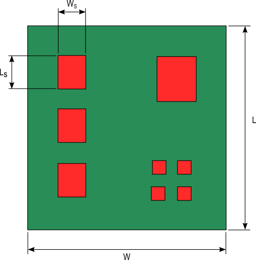
Figure 1. PCB with heat generating components
This method calculates the temperature distribution of a circular heat source on an infinite surface that is convection cooled. Since almost all heat generating components on a PCB are rectangular in shape a circular source of equal area is used to represent the heat generating component. The equivalent radius is given by equation 3.

Equations 4 and 5 calculate the temperature rise at any point, P on the infinite surface measured radially from the center of the heat source, to a distance d as depicted in figure 2.
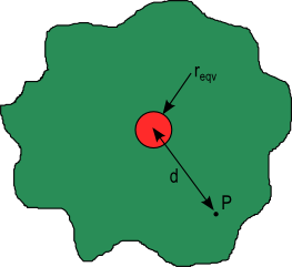
Figure 2. Infinite plate with a circular heat source


Qs is the heat generated by the heat source that flows into the PCB and t is the thickness of the PCB. The constants C1 and C4 are calculated from equations 7 and 8. Variables I0, K0 are modified Bessel functions of the first and second kind respectively, of order 0 and α is given by equation 6.


where:


The next step is to use the temperature rises that are calculated with equations 4 through 8 for an infinite plate to calculate those of a finite rectangular plate representing the PCB. This is done by a process of mirroring as shown in figure 3. Plate 1 in the center represents the PCB. The temperature rise at any location on plate 1 is obtained by a summation of the temperature rise contributions from all the mirrored heat sources including the heat source on plate 1. Figure 3 shows two mirroring operations, plates 2 to 9 and plates 10 to 25. Increased accuracy is achieved as the number of mirroring operations are increased. For most PCBs 1 to 2 mirroring operations provides acceptable accuracy.
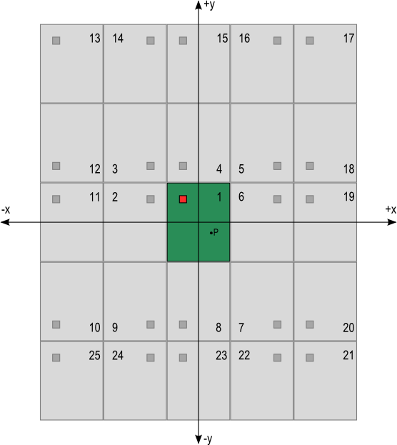
Figure 3. Mirrored heat sources to determine the heat source temperature
Equations 9 through 17 are the distances from the center of the heat sources in the first mirroring operations (plates 1 through 9) to a point P on the center plate, plate number 1. The x and y variables with subscripts s and p are the coordinates of the mirrored heat source and the point P respectively referenced from the coordinate axes shown in figure 3.


The temperature rise for each source at the corresponding distance d is calculated using equations 4 through 8. The resulting temperature rise values are added together to determine the temperature rise ΔTP at the point P as shown in equation 18. The procedure is similar as the number of mirrored heat sources are increased.

The subscript N is the number of mirrored heat sources including the heat source on the center plate.
Equations 4 through 7 assume heat transfer is taking place from only one side of the PCB. To evaluate cooling from both sides of the PCB the effective convection coefficient heff is multiplied by 2.
If there are more than one heat sources attached to the PCB the principle of superposition is used to determine the temperature of a location P on the surface of the PCB by taking into account the influence of each heat source at that point. For each heat source calculate the temperature rises at the location of P and then sum the temperature rise contributions at point P. The summation of the temperature rises at point P for a PCB that has M heat sources and N mirrored heat sources can be written mathematically as:

The temperature rise at the base of a component mounted to a PCB can simply be determined by calculating the temperature rise a point P located at the center of the component. The temperature at the base of the component, ΔTb is then used to calculate the component junction temperature using equation 20.

where:

The junction to board thermal resistance, θjb is a tested value provided by the component manufacturer.
This calculation methodology has one major draw back. The use of a circular heat source to approximate a rectangular heat source will introduce increasing error as the aspect ratio of the heat source (Ls/Ws) deviates from a value of 1. Oblong heat sources can be more accurately modeled by subdividing the component shape into smaller areas that have an aspect ratio of 1. See figure 4.
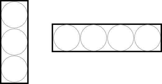
Figure 4. Approximation of oblong heat sources by subdivision
PCB Trace Temperature Rise
The first step to estimate the temperature rise of a trace is to determine the heat generated by the trace, Ptrace. This is calculated using equation 21.

The resistance, Rtrace of the trace is temperature dependent and is given by equation 22 and I is the current flow through the trace.

where:


Typical values for copper traces at a reference temperature of at 20°C are:


Note, equation 22 does not calculate power loss caused by skin effects typically seen in high frequency applications. Because the thickness of most traces are very small the skin effect is pronounced only at extremely high frequencies.
The most accurate method to determine the trace temperature is to analyze the trace using multiple circular heat sources as shown in figures 2 and 4 and described in the previous section. For relatively short traces the number of calculations needed are manageable if using a spreadsheet since a reasonable number of circular heat sources can be used to approximate the entire trace. For long traces a simplified method can be used to provide a good estimation of trace temperature.
The simplified trace temperature calculation method divides the circuit board into two sections as shown in figure 5. The thermal resistances from the trace to the ambient associated with each section are calculated and combined to determine an overall trace to ambient thermal resistance. Section A is approximated as an extended surface similar to a fin on a heat sink. The trace to ambient thermal resistance RA associated with section A is given by equation 23.
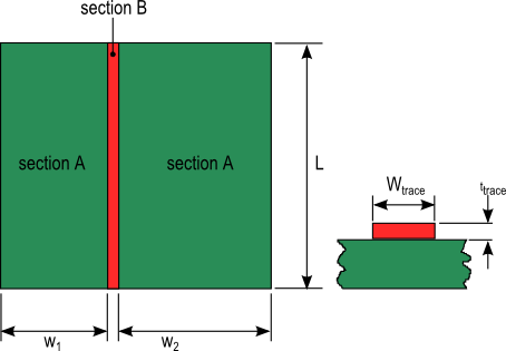
Figure 5. Sections used to approximate trace to ambient thermal resistance

η1 and η2 are extended surface efficiency values that are calculated using equations 24 and 25 respectively. Areas A1 and A2 are the rectangular areas of section A corresponding to w1 and w2.


where m is given by:

The trace to the ambient thermal resistance associated with section B is calculated by considering the combination of the conduction thermal resistance of heat flowing from the bottom of the trace through the PCB and the convection/radiation thermal resistance of the heat flowing from the top of the trace and the bottom of the PCB. The total thermal resistance for section B, RB is calculated using equations 27 through 29.


Thermal resistances RA and RB are parallel resistances. The total thermal resistance from the trace to the ambient and the average trace temperature is given by equations 30 and 31 respectively.


Example Calculations
The calculation process explained previously is used to determine the junction temperature rises of two MOSFETs mounted to a 300mm X 300mm PCB with a thickness of 4mm. The MOSFETs are labeled A and B in figure 6. Table 1 lists the size, location, heat loss and junction to board thermal resistances for the devices.
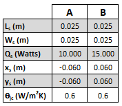 Table 1. Parameters for the MOSFETs attached to the PCB temperature rise calculation example
All of the heat loss is assumed to be conducted into the PCB. The PCB is cooled via natural convection and radiation from the top and bottom surfaces with an effective convection coefficient, heff of 15 W/(m2K). The effective thermal conductivity, keff of the PCB is 54 W/(mK).
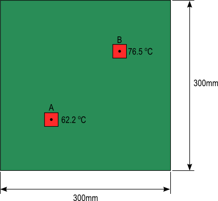
Figure 6. PCB layout and dimensions of calculated example
A MSExcel spreadsheet is used to conduct the calculations. Two calculation tables are created in the spreadsheet as shown in figure 7.
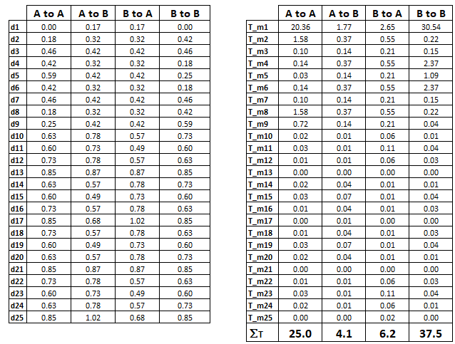
Figure 7. Tables used to calculate MOSFET temperature rises
The first table contains the calculated distances of the mirrored heat sources for 2 mirroring operations to the center of the MOSFETs A and B. The second table uses the corresponding distances to determine the temperature rise due to each mirrored source at the locations of the MOSFET’s. The temperature values in each column are summed. The sum of the values in column “A to A” are added to that of column “B to A” to determine the temperature rise of surface of the PCB located beneath MOSFET A. Equation 20 is then used to calculate the junction temperature of the MOSFET A. The same is done with columns “A to B” and “B to B” to calculate the junction temperature of MOSFET B. The results are shown in figure 6.
An online calculate that will estimate the temperature rise of a PCB and the junction temperature of a component attached to the PCB is available free of cost. Click the following link: PCB Temperature Calculator
