Thermal management is a crucial aspect of designing and manufacturing electronic devices, as heat generated by the components can lead to performance issues and even device failure. To ensure the reliable and efficient operation of electronic devices it is essential to understand how to effectively dissipate heat away from the heat generating devices. These heat generating components are often mounted on printed circuit boards (PCBs) which in many cases are used as a heat sink to cool the attached component.
Thermal resistance is a measure of how well a material or device transfers heat to its surroundings and is often used to predict the thermal performance of a PCB and to calculate the temperature of the attached component. This technical article will provide a detailed explanation of the formulas and method used to calculate the thermal resistance of a PCB. The calculation methodology will take into account the PCB insulation (FR4)/copper layer thicknesses, percent copper coverage in each layer, location of these layers with respect to the heat generating component and usage of thermal vias.
Layout and structure of the PCB
A PCB consists of alternating layers of dielectric and conductive materials typically made using FR4/resin and copper respectively as shown in figure 1. Layers that are used for ground planes often are 100% conductive material. While the layers with attached components, traces and interconnects will have some mixture of conductive and dielectric materials.
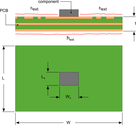
Figure 1. PCB layout
The preceding calculation procedure assumes that the component is intimately attached to the PCB using an exposed metal pad or some similar attachment method that creates an extremely low thermal resistance path between the component and the PCB. The component is located at or close to the geometric center of the PCB. The upper and lower surfaces of the PCB are cooled via natural convection or forced convection and radiation. A heat transfer coefficient hext is used to quantify the effectiveness of cooling from these outer surfaces. Reference the articles How to design a flat plate heat sink and Performance of a LED flat plate heat sink in multiple orientations for the formulas used to calculate hext for natural convection and radiation.
Calculating the thermal resistance of each PCB layer
To facilitate the preceding calculations the rectangular PCB and attached component are converted to circles of equivalent areas with radii ro and ri respectively using equations 1 and 2. The approximation of the rectangular areas as circular areas introduces an error of less than 1% at an aspect ratio (width/length) of 1, increasing to an error 8% at aspect ratios of 2.5 or 0.4.


The composite nature of the PCB complicates the thermal analysis and does not allow for the PCB to be treated as a simple flat plate heat sink made from uniform thermal conductivity material. The thermal conductivity through the thickness and in the plane of the PCB are different. Additionally, the position of the dielectric and conducting layers from top to bottom affect how well heat is conducted from the heat generating component through the PCB and then to the surroundings.
The thermal resistance calculation is conducted layer by layer to account for the non-uniform thermal conductivity of the PCB. The section of each layer directly under the component is a disk with radius ri and thickness tn. This disk will be referred to as the “inner disk”. The periphery of the disk has an equivalent convection coefficient ho,n that represents the effective cooling of the outer portion of the layer as shown in figure 2.
The subscript n in tn , ho,n and all other variables subsequently defined refers to the layer number where layer number 1 is attached to the component and N is the total number of layers in the PCB.
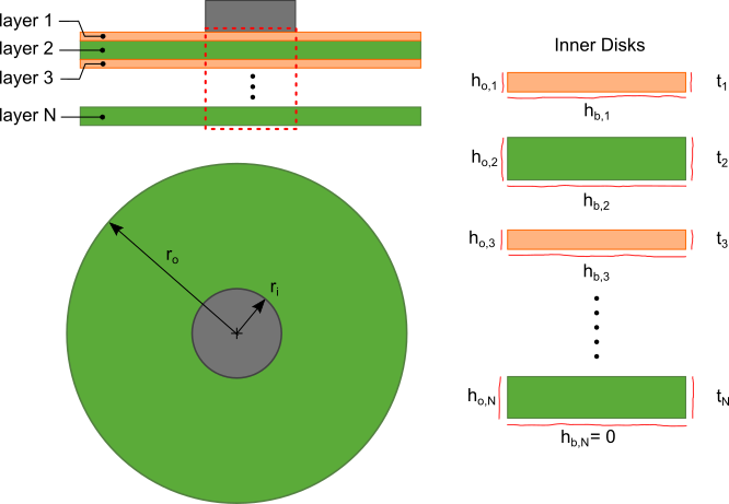
Figure 2. PCB layers and sections used in the analysis.
The outer portion of each layer is an annulus (referred to as the “outer annulus”) with inner and outer radii ri and ro respectively.
The calculation for ho,n is developed with the approximation that the temperature difference between the layers of the PCB is small. As such the flow of heat is predominantly radial in the outer annulus. The resistance to heat flow in the outer annulus can then be approximated by the thermal resistance network shown in figure 3.
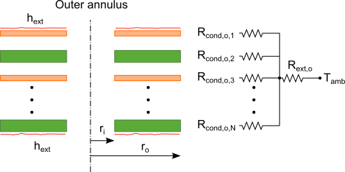 Figure 3. Outer annulus layers and resistance network
Rcond,o,n in the thermal resistance network shown in figure 3 represents the conduction thermal resistance of each layer and Rext is the thermal resistance due to the convection/radiative cooling hext on the exposed upper and lower surfaces of the PCB. The total equivalent thermal resistance of the thermal resistance network is determined by combining the parallel and series resistances as illustrated in figure 4.

Figure 4. Simplified thermal resistance network for the outer annulus layers
To determine Rcond,o,n for each layer, Router is first calculated by determining keff, the average in-plane thermal conductivity of the PCB. keff is an average of the effective thermal conductivity of each layer, keff,n.
The effective thermal conductivity keff,n of each layer is:

where:


The value of σc,n ranges from 0 to 1. It can be determined by estimating the conductor coverage area on each layer and dividing that value by the total PCB area (L x W).
Thermal conductivities of 398W/m·K for copper and 0.3W/m·K for FR4 are most often used for the conductor and dielectric materials respectively.
The average in-plane effective thermal conductivity of the entire PCB, keff is:

The resistance Router is calculated using the solution for a circular fin [1] expressed as:

where:


The multiplication of hext by 2 in equation 6 indicates that both the upper and lower surfaces of the PCB are subjected to convective and/or radiative cooling.
The use of Bessel functions in equation 5 may seem complex, however Bessel functions are readily available in MS Excel or any commercial mathematics software as a built-in function.
With the value of Router known, Rcond,o,n for each layer is calculated using equations 7, 8, 9 and 10.


Aext is the exposed surface area of the outer annulus.

The equivalent convection coefficient on the periphery of the inner disk for each layer ho,n can now be calculated with equation 11.

Combining the PCB layer thermal resistances
The next step in the calculation is to determine the value of hb,n, the effective heat transfer coefficient acting on the base of the inner disk of each layer as shown in figure 2. This is done by calculating the equivalent heat transfer coefficient that the inner disk of the nth layer applies to the lower surface of the inner disk of the n-1 layer. Equation 12 uses the equation for an extended surface with convection heat transfer around the periphery and lower surface [2] to calculate hb,n-1.

As and Ps are the cross-sectional area and perimeter respectively of the inner disk.


The calculation is started at the last (Nth) layer with hb,N=0 on the bottom surface of the inner disk for that layer. hb,N is not set to equal hext since the dissipation of heat from the base of the inner disk will be evaluated separately.
Using equation 12, hb,N-1 is calculated. This process is repeated N times for all the layers resulting in an equivalent heat transfer coefficient hb. This process is illustrated in figure 5.
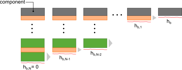
Figure 5. Iterative calculation for hb
The heat transfer coefficient hb is the equivalent heat transfer coefficient of the conduction resistance due to flow of heat through the inner disk and into the outer annulus of the PCB acting on the heat generating component. This conduction thermal resistance is:

Note: R*cond,o includes the thru-plane and in-plane conduction across the PCB which is why the “*” notation is used to differentiate this variable from Rcond,o which only accounts for the in-plane conduction in the outer annulus.
The heat flow from the heat generating component through the PCB to the ambient is represented by the thermal resistance diagram in figure 6. Flow through the bottom of the inner disk exposed to hext is accounted for with Rcond,i and Rext,i thermal resistances.
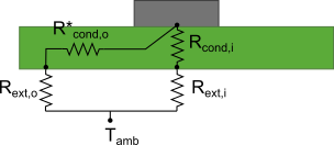
Figure 6. Thermal resistance network for heat flow through the PCB to the ambient
Rcond,i is the summation of the thru-plane thermal resistances of each layer, (equation 17) and Rext,i is the thermal resistance due to hext of the area As.


The thermal resistances in figure 6 are combined to a single thermal resistance Rpcb:

Thermal via calculations
Thermal vias placed under the heat generating component provide a path to more efficiently transfer heat from the heat generating component to the inner layers and base layer of the PCB. This then allows to the heat to be spread across these layers reducing the thermal resistance of the PCB.
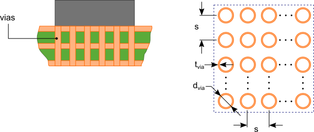 Figure 7. PCB with thermal vias
The analysis of the effect of imbedded thermal vias as shown in figure 7 requires the calculation of an equivalent through-plane thermal conductivity, kvia,n for the inner disk of each layer. This is calculated by evaluating the flow of heat through the inner disk of each layer through three parallel thermal resistances:
- Rbarrel, the thermal resistance of the barrel of the thermal via.
- Rfiller, the thermal resistance of the filler material of the via if any.
- Rmatl,n, the thermal resistance of the layer material surrounding the thermal via in the s x s square region shown in figure 7.


kbarrel and kfiller are the thermal resistances of the thermal via barrel and filler material respectively.
The thermal resistance of the entire s x s, cell, Rcell,n for each layer is:

If the thermal via is not filled then the 1/Rfiller term in equation 24 is omitted.
The equivalent thermal conductivity of each layer of the inner disk with thermal vias is then:

In equations 12, 15 and 17, keff,n is replaced with kvia,n and Rpcb is calculated for a PCB with vias under the heat generating component.
Junction to ambient thermal resistance calculations
Rpcb is the thermal resistance from the base of the component to the atmosphere. To determine the junction to ambient thermal resistance, the junction to board thermal resistance typically listed as Θjb or Rjb in the component literature is added to Rpcb. The temperature of the junction, Tj can now be determined using equation 26.

Tamb is the external ambient temperature and Qs is the heat generated by the component.
This calculation excludes any heat loss from the top of the component exposed to the atmosphere. Typically, this heat loss is small when compared to the heat dissipation from the PCB. If there is a heat sink attached to the component, then the heat loss through the heat sink is significant and must be considered. Figure 8 shows the thermal resistance network for the PCB with a heat sink of thermal resistance Rhs, attached to the component. Rjc is the junction to case (top) thermal resistance.

Figure 8. Thermal resistance network for the PCB
Calculating for the junction temperature, Tj from this thermal resistance network yields:

An online PCB temperature calculator that uses the calculation procedure outlined in this blog post is available free of cost. Click the following link: PCB Temperature Calculator.
References
[1] F. Incropera, D. DeWitt, (2011). Fundamentals of Heat and Mass Transfer (7th ed.). Hoboken: Wiley. p124
[2] F. Incropera, D. DeWitt, (2011). Fundamentals of Heat and Mass Transfer (7th ed.). Hoboken: Wiley. p118, table 3.4
